Techniques of using magnetic field loops
by Dr. Min Zhang, the EMC Consultant
Measurement
Positioning
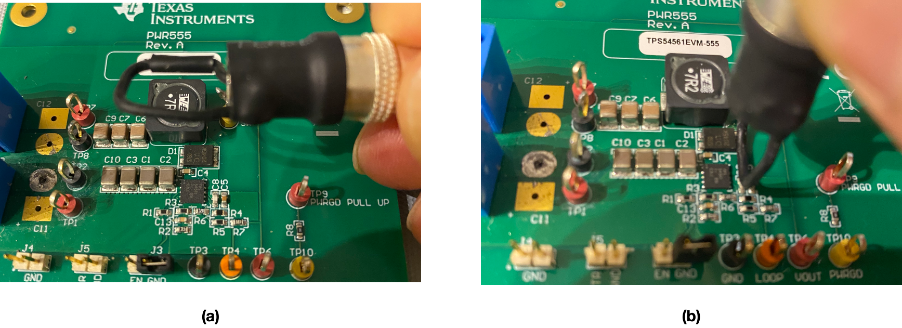
There are two ways of positioning a magnetic field loop over a PCB. When positioned horizontally to the PCB (shown in Figure 6 (a)), a magnetic field loop picks up the changing magnetic field using the whole loop area. This is what the EMC engineers called “sniffing”. The purpose is to identify the “hot” area (maximum changing magnetic field area) on the PCB. The magnetic field loop can be connected either to a spectrum analyzer or an oscilloscope with 50 ohm impedance. The “hot” area is identified when the results on the scope/spectrum analyzer shows maximum values during the “sniffing” exercise.
When positioned perpendicularly to the PCB (shown in Figure 6 (b)), a magnetic field loop is used to measure the induced voltage on a particular trace/track on the PCB. The reason that the loop needs to be placed perpendicularly is to minimize the induced voltage on the side wires of the loop. In this case, the magnetic field loop should be connected to a high bandwidth oscilloscope as the measurement is in the time domain.
Demonstrations
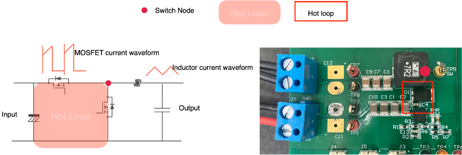
For a typical buck converter, the current waveforms of the switch side and the load side are shown in Figure 7. Both the switch node and the “hot loop” area are shown. A Texas Instrument buck EVM board is used for demonstration purposes.
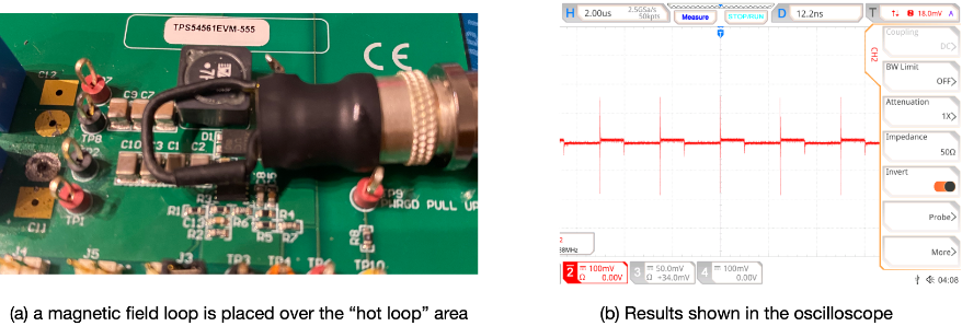
Moving a magnetic field loop horizontally over the PCB, one can easily identify the “hot loop” area. In Figure 8, the induced peak to peak voltage reached 300 mV for a small magnetic field loop, indicating a sharp rise time during the hard switching events. If one were to integrate the result, a current waveform similar to that is shown in Figure 7 (the MOSFET current waveform) can be arrived at. Remember, the magnetic field loop outputs a voltage reading (V=Mdi/dt). To get the current waveform, one need to do an integration.
I=1/M∙∫Vdt
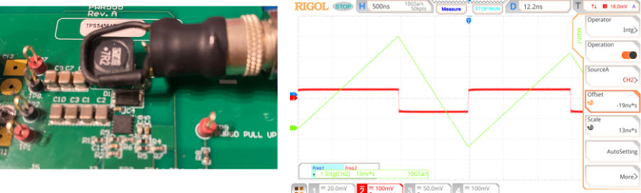
Similarly, when placing the loop over the inductor, a smooth voltage waveform is seen as shown in Figure 9. Using the integration function in the oscilloscope, one can calculate the inductor current waveform (shown in green triangular waveform in Figure 9).
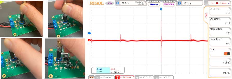
After the “hot loop” area is identified, the next step is to place the magnetic field loop perpendicularly to the PCB and move it slowly across the suspicious area. Note down areas where large voltage spikes are seen during the exercise. Because the area on the PCB is rather small, a smaller size shielded loop is used instead. A few areas on the PCB were probed, all showed similar induced voltage level as shown in Figure10.
Can we predict the EMI results based on this technique?
This is basically asking if there is any correlation between the near-field measurement and far field measurement result. And the answer is no. Any attempt to use the near field measurement to predict far field performance would lead to either under-estimation or over-estimation. Thus the proposed technique in this article is most suited for a few scenarios listed below:
- If a product/system is known to have failed EMC test, using a magnetic field loop can quickly help locate the noise source and propagation mechanism.
- If a probe is well calibrated, then using the loop might give you a Pass/Fail indication.
But how to calibrate a homemade magnetic field loop? Since each loop is made differently in size. For shielded magnetic field loops, the diameter of the coaxial also plays a role in affecting the mutual inductance. Many factors could affect the reading of a magnetic field loop. Therefore, the loop method result should only be treated as a qualitative indicator.
One method the author often uses is to test the loop on a known product. For instance, both the conducted and radiated emission test results of the EVM board in this study were known to the author. Therefore, for products that need to pass the automotive EMI test standards such as those defined in CISPR 25, any induced voltage over 100 mV on a small magnetic field loop certainly will raise a red flag. If the product is a home appliance product, then even 200mV induced on the same loop will most likely be okay.
References
[1] D. C. Smith, High Frequency Measurements and Noise in Electronic Circuits, New York: Van Nostrand Reinhold, 1993.
[2] Doug Smith, Arturo Mediano, “Shielded vs unshielded square magnetic field loops for EMI/ESD Design and Troubleshooting,” InCompliance Magazine, vol. July, no. July, 2014.