Filter Layout

by Dr. Min Zhang, the EMC Consultant

Mach One Design EMC Solutions

Here is a classic question; – where should we put the filter with regard to the noise source? Shall we place the filter close to the noise source or away from it? The answer is; – if you can, you should always place the filter in a quiet environment, i.e. away from the noise source. 

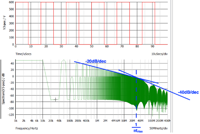
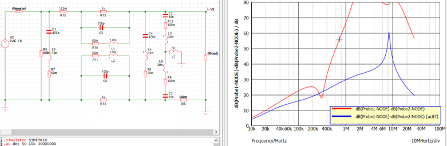
Here we should not get confused with what we say about ‘solving EMI problems at the noise source’. We all know that the best approach to solving EMI problems is to suppress the noise source. Without understanding the principles, engineers often put an EMI filter close to the noise side, such as a SMPS on a PCB, or a line filter close to a motor drive circuit. This creates problems because the strong leakage field of the noise source will couple strongly with the passive components of a filter. As a result, a carefully designed filter, which is supposed to give 60-80 dB attenuation according to the simulation/calculation, often ends up having only 10-20 dB insertion loss. This is particularly true when the frequency increases. 

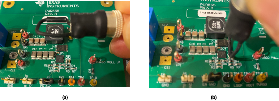
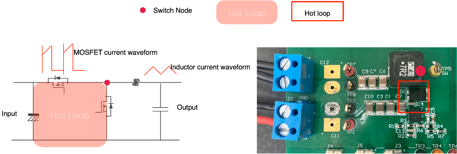
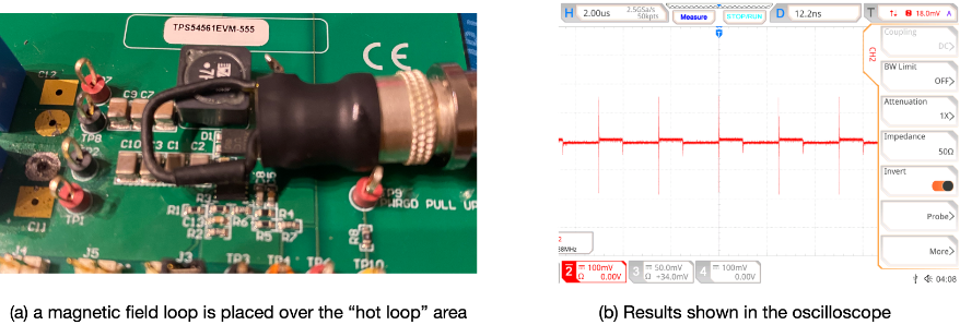
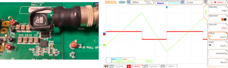
The circuit shown in Figure 1 is given to demonstrate the point. The input stage of a typical buck converter using in integrated switching IC is shown. On the input side, the filter stage is separated from the input capacitors by including the red dashed line. Note that there can never be a strict separation line between the filter and the input capacitors as the input capacitors also provide a low impedance path to noise, so they work nicely with the filter. But here the two are separated to make the point.

Figure 1 The input stage of a typical integrated buck converter

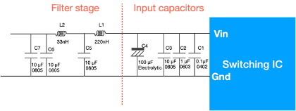
The input capacitors are part of the SMPS design. Therefore, one will need to design the capacitors to make sure there is always enough energy delivered in the most efficient way whenever the switch is turned on. This is often achieved by the following: 

  1. Populate the input supply rail with several decoupling capacitor sizes (0402, 0603, 0805, etc) so that energy is available over a wide frequency spectrum.   
  2. The decoupling capacitors should be connected as close as possible to the Vin pin. 
  3. Locate the smallest size capacitor (in this case C1, 0402) first to the Vin pin.
  4. The electrolytic capacitor C4 serves as the main energy storage device, but it also provides damping of the system due to its relatively larger ESR.
  5. If the electrolytic capacitor has a metal housing, such as aluminium, due to the larger size of the electrolytic capacitor, the metal housing also serves as a shield to block some of the electric field created by the SMPS. 

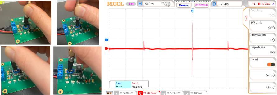
The filter stage is designed as a multi-stage filter which consists of two inductors and a few ceramic capacitors. The red line shown in Figure 1 indicates that there must be a distance between the filter and the input capacitors. This is to avoid field coupling and make the input filter stage more effective. On a PCB level, this is often achieved through the following steps:

  1. Put the input filter away from the noise source, if the noise source is a SMPS and it is located on one side of the PCB, the safe side of a filter should be on the opposite side of a PCB.
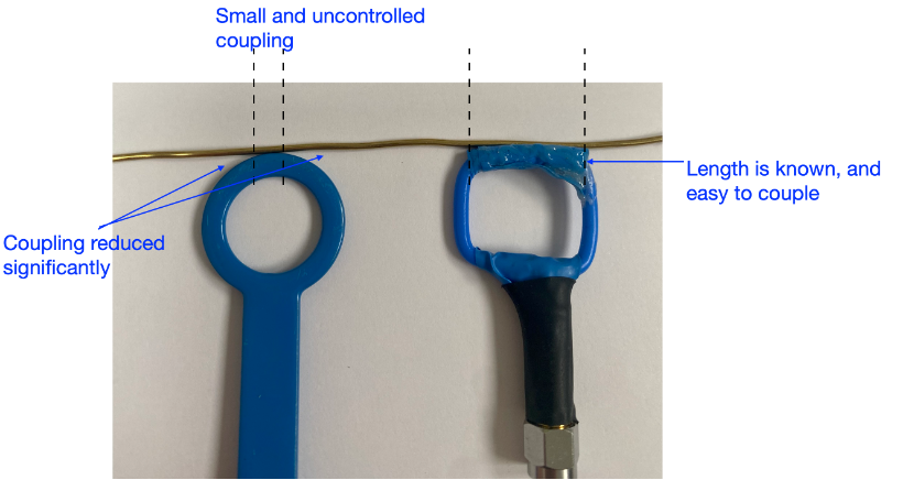
  2. If the filter stage has to be on the same side of the SMPS, a physically long distance shall be kept. The distance depends on the strength of the leakage field of the SMPS. For instance, if the switch node of the SMPS is kept quiet by a shield, then the distance between the filter and SMPS can be shortened.
  3. The connection between the filter stage and the input capacitors should always be a high impedance path such as an inductor (L1 shown in Figure 1).

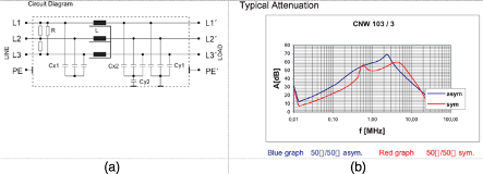
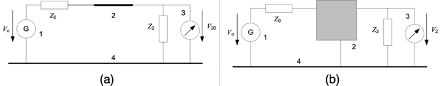
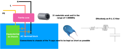
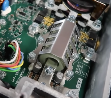
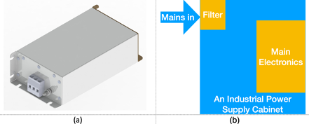
The same principle applies to much larger systems such as an industrial motor drive system or power supply. For instance, a line filter used for an industrial motor drive application such as the one shown in Figure 2 (a) is always much more effective if it is placed near the mains entry point of the cabinet, i.e. to keep the mains wiring and the line filter far away from other wiring and harnessing inside the cabinet. Again, the reason is to avoid close field coupling between the noise source and the filter component. 

Figure 2 (a) a line filter made by REO, (b) best location for such a filter to be effective

Training

If you want to learn more about EMC and become an expert in troubleshooting EMI problems. Why not attend our video training course? Priced from $199, you can get 10 hour lessons. Check https://mach1design-shop.fedevel.education/itemDetail.html?itemtype=course&dbid=1644339825702&instrid=us-east-2_4pKkzzNo1:fe56227a-47c8-4ea8-ba6f-2930d01d7db8

Design Filters with Simulation

by Dr. Min Zhang, the EMC Consultant

Mach One Design Ltd

Most of the noise that engineers come across in the field is generated by high-frequency, fast switching devices. Typical examples are motor drive inverters, DC-DC converters, power supplies, microcontrollers and communication chips. Therefore, filters are often designed to suppress the noise caused by switching events. 

In the past, IGBTs and MOSFETs were the main switches. MOSFETs were predominantly used in low voltage applications while IGBTs were used in medium voltage applications. When the voltage is above 800V, IGCTs and GTOs are the devices of choice. MOSFETs can be switched rather quickly, but they are limited by the voltage rating and their thermal properties, therefore, typically they are limited to about 150kHz switching frequency and the rise time is often found to be from a few nanoseconds to 10s of nanoseconds. IGBTs have a tail-current, which limits their switching speed and switching frequency. Typically, the switching frequency of an IGBT based system is limited to about 60kHz. 

This will soon change as the newly developed wide-band-gap (WBG) devices such as Silicon-carbide (SiC) and Gallium-nitride (GaN) devices show superior performance over the MOSFETs and IGBTs. The fact that they can switch faster at higher voltage means the dV/dt of WBG devices is a lot higher. This inevitably leads to more EMI. 

There are two aspects of a switching event, the switching frequency and the switching speed. When talking about EMI associated with the switching events, many engineers often focus on the switching frequency and overlook the impact of switching speed. The switching speed should have more attention paid to as it is the main EMI source. It is not necessary to have a high switching frequency to cause EMI problems. Consider this example; an electrostatic discharge (ESD) event does not have MHz of switching frequency, but the rise time is as short as 10s-100s of picoseconds. One ESD event could potentially radiate the energy to a nearby system and cause trouble.

A switching event is simulated in the SPICE simulation software. The simulated switching event has a 60kHz switching frequency, with 600V DC voltage, and the duty ratio in this case is 50%. The rise time is set as 12 ns to give a 5V/ns switching speed. Spectrum analysis of the switching event is shown in Figure 1. 

Figure 1 Spectrum of a 60kHz switching event with a rise time of 5V/ns

Notice that the -20dB/decade line and the -40dB/decade line crosses at the frequency point of 1/πtrise, which in this case is calculated to be 26.5MHz. Ideally, one would like the -40dB/decade roll off to occur at a lower frequency point, because the noise spectrum decreases a lot faster after this crossing point. But the roll off point only depends on the rise time of a switching event. 

Engineers often don’t have the option of shifting this point. This is because the rise time of a switching event often cannot be increased as increased rise time leads to more switching loss and less system efficiency. 

To demonstrate the effect of sharp rise time, in Figure 2, a faster rise time (10V/ns) is simulated for comparison. As it can be seen, every time the switching speed is doubled, it results in a 3-6dB noise increase from 1/πtrise

Figure 2 10V/ns rise time spectrum (blue) vs 5V/ns rise time (green)

Once the spectrum characteristics of a switching event are understood, it is then easy to design a filter that aims to suppress the noise at the frequency range of interests. 

For instance, a motor drive causes conducted emission between 100 kHz to 10 MHz, the lower frequency range noise (<1MHz) often needs differential mode filtering, whereas, between 1MHz and 10 MHz, some form of common-mode filtering is needed. A three-phase filter that has sufficient attenuation in this range would be a good choice. One example is a C-L-C (π) filter, which is shown in Figure 3. 

Figure 3 REO CNW 103 three-phase filter gives good attenuation in the lower to mid frequency range

Training

If you want to learn more about EMC and become an expert in troubleshooting EMI problems. Why not attend our video training course? Priced from $199, you can get 10 hour lessons. Check https://mach1design-shop.fedevel.education/itemDetail.html?itemtype=course&dbid=1644339825702&instrid=us-east-2_4pKkzzNo1:fe56227a-47c8-4ea8-ba6f-2930d01d7db8

Understanding Insertion Loss

by Dr. Min Zhang, the EMC Consultant

Mach One Design EMC Solutions

Filters are almost always a part of an electronics design. Design engineers design a filter to achieve certain attenuation in a specified frequency range. We have seen that with inductive components, the impedance increases with frequency while the capacitors’ impedance decreases with frequency. By combining inductors and capacitors, we can build many types of filters, such as high-pass, low-pass or band-pass. Popular filter configurations include L-C, C-L-C (π) or L-C-L (T).

The performance of a filter is measured in terms of attenuation, or insertion loss, both of which use the units of decibels (dB). The best place to start this discussion is CISPR 17, which defines the technical terms of a filter. It also presents a detailed explanation of how to measure the insertion loss of a filter. 

A filter often provides attenuation to noise in both differential mode and common mode. At a low frequency range (often between a few kHz and 1 MHz), noise is predominantly a differential mode mechanism. When the frequency goes up, common mode noise becomes more dominant. 

Take a 50Ω/50Ω (source impedance/load impedance) system for instance, CISPR 17 defines two tests to measure the filter performance, which are symmetrical (differential mode) and asymmetrical (common mode). The test set-ups are shown in Figure 1. The signal generator (G) performs a signal sweep between the defined frequency range. The voltage across the load (Z2) is measured during the sweep.

Figure 1 Test set-up for insertion loss, CISPR 17 (a) symmetrical test, (b) asymmetrical test

Note that in both cases Zand Z2 are 50 Ω. In reality, a 50Ω/50Ω system rarely exists. Therefore, the worst-case test set-ups, such as 0.1Ω/100Ω and 100Ω/0.1Ω give better filter performance analysis. 

The insertion loss is defined as 

Insertion Loss = 20log(V20/v2)

Where V20 is the voltage across Z2 before the filter is inserted, and V2 is the voltage measurement after the filter is inserted, as per Figure 2.

Figure 2 Test circuits for insertion loss measurement, CISPR 17 (a) reference, (b) filter

While it sounds easy and straight forward, engineers often need to see the test set-up to understand the concept better. Figure 3 shows the test set-up of an REO filter according to CISPR 17. The circuit diagram of the filter being tested is shown in Figure 4(a) and the insertion loss curve is shown in Figure 4(b). 

Figure 3 Test set-up for filter insertion loss
Figure 4 (a) Circuit diagram and (b) typical attenuation of a REO single phase mains filter

A simulated filter model is built in the SPICE simulation tool and the circuit can be found in Figure 5. As shown, when introducing parasitics into the simulation model, a close to real measurement result can be achieved. To build a useful simulation model, especially before the filter is implemented, engineers need to understand the parasitics of each passive component in the filter. If the passive components are arranged so that coupling occurs, engineers should also be aware that the filter performance could be compromised by coupling. If an off-the-shelf filter is purchased, it is a good idea to always ask the filter manufacturer for a measured attenuation curve such as the one shown in Figure 4. 

Figure 5 Simulation model shows a close-to-measurement attenuation curve

Training

If you want to learn more about EMC and become an expert in troubleshooting EMI problems. Why not attend our video training course? Priced from $199, you can get 10 hour lessons. Check https://mach1design-shop.fedevel.education/itemDetail.html?itemtype=course&dbid=1644339825702&instrid=us-east-2_4pKkzzNo1:fe56227a-47c8-4ea8-ba6f-2930d01d7db8

Advanced Implementation of Ferrite Cores

by Dr. Min Zhang, the EMC Consultant

Mach One Design

One of the challenges with filters are the cost associated with high voltage and high current filter components. When the current rating exceeds 10s of amperes, the magnetic components become costly. 

One way of implementing a cost-effective filter is to utilise magnetic cores. The ferrite cores introduced previously are just one example. Of course, the core material could be nanocrystalline or others depending on the application. Figure 1 demonstrates this concept. A ferrite, together with Y-capacitors form an R-L-C filter for the common-mode noise. The great virtue of this configuration is that the core is not subjected to saturation, so it is suitable for high current application. 

Figure 1 A low-cost filter implementation using ferrite cores and Y-capacitors

Magnetic cores are seen in many applications, such as the DC-DC converter used in Tesla electric vehicle (shown in Figure 2). The output current for this type of application often reaches beyond hundreds of amperes, any inductors on the output would be bulky, heavy and costly. Instead of placing inductors, the positive and negative rails were put on adjacent layers of the board. Depending on the current rating, often wide track or plane were used. Similar to a bifilar winding, all the magnetic field then flows in the small gap between the two planes and the only remaining flux is the high frequency common mode noise. All one needs to do then is to put a core (or multiple cores) through the board or around the board. Mechanically, this is also easy to do. 

Figure 2 A DC-DC converter used in Tesla electric vehicles, multi-cores were clamped in the 12V DC output bus bar. The current rating of the output could be as high as 250 Amps

Training

If you want to learn more about EMC and become an expert in troubleshooting EMI problems. Why not attend our video training course? Priced from $199, you can get 10 hour lessons. Check https://mach1design-shop.fedevel.education/itemDetail.html?itemtype=course&dbid=1644339825702&instrid=us-east-2_4pKkzzNo1:fe56227a-47c8-4ea8-ba6f-2930d01d7db8

The Magic Loop – Part 3

Techniques of using magnetic field loops

by Dr. Min Zhang, the EMC Consultant

Mach One Design

Measurement

Positioning

There are two ways of positioning a magnetic field loop over a PCB. When positioned horizontally to the PCB (shown in Figure 6 (a)), a magnetic field loop picks up the changing magnetic field using the whole loop area. This is what the EMC engineers called “sniffing”. The purpose is to identify the “hot” area (maximum changing magnetic field area) on the PCB. The magnetic field loop can be connected either to a spectrum analyzer or an oscilloscope with 50 ohm impedance. The “hot” area is identified when the results on the scope/spectrum analyzer shows maximum values during the “sniffing” exercise. 

When positioned perpendicularly to the PCB (shown in Figure 6 (b)), a magnetic field loop is used to measure the induced voltage on a particular trace/track on the PCB. The reason that the loop needs to be placed perpendicularly is to minimize the induced voltage on the side wires of the loop. In this case, the magnetic field loop should be connected to a high bandwidth oscilloscope as the measurement is in the time domain.

Figure 6 Positioning of a magnetic field loop over a PCB (a) horizontal position to “sniff” (b) perpendicular position to measure induced voltage on a trace

Demonstrations

For a typical buck converter, the current waveforms of the switch side and the load side are shown in Figure 7.  Both the switch node and the “hot loop” area are shown. A Texas Instrument buck EVM board is used for demonstration purposes. 

Figure 7 The “hot loop” area in a buck converter

Moving a magnetic field loop horizontally over the PCB, one can easily identify the “hot loop” area. In Figure 8, the induced peak to peak voltage reached 300 mV for a small magnetic field loop, indicating a sharp rise time during the hard switching events. If one were to integrate the result, a current waveform similar to that is shown in Figure 7 (the MOSFET current waveform) can be arrived at. Remember, the magnetic field loop outputs a voltage reading (V=Mdi/dt). To get the current waveform, one need to do an integration. 

I=1/M∙∫Vdt

Figure 8 Placing a magnetic field loop horizontally over the PCB and move along the loop until the maximum induced voltage is seen in the oscilloscope 

Similarly, when placing the loop over the inductor, a smooth voltage waveform is seen as shown in Figure 9. Using the integration function in the oscilloscope, one can calculate the inductor current waveform (shown in green triangular waveform in Figure 9).

Figure 9 Placing the loop over the inductor gives the induced voltage caused by current going through the inductor. The integration of the waveform gives the inductor current waveform

After the “hot loop” area is identified, the next step is to place the magnetic field loop perpendicularly to the PCB and move it slowly across the suspicious area. Note down areas where large voltage spikes are seen during the exercise. Because the area on the PCB is rather small, a smaller size shielded loop is used instead.  A few areas on the PCB were probed, all showed similar induced voltage level as shown in Figure10. 

Figure 10 Use a smaller size loop and place it perpendicularly on the PCB, traces/tracks where large di/dt can thus be measured, the result is shown here. 

Can we predict the EMI results based on this technique?

This is basically asking if there is any correlation between the near-field measurement and far field measurement result. And the answer is no. Any attempt to use the near field measurement to predict far field performance would lead to either under-estimation or over-estimation. Thus the proposed technique in this article is most suited for a few scenarios listed below:

  1. If a product/system is known to have failed EMC test, using a magnetic field loop can quickly help locate the noise source and propagation mechanism.
  2. If a probe is well calibrated, then using the loop might give you a Pass/Fail indication. 

But how to calibrate a homemade magnetic field loop? Since each loop is made differently in size. For shielded magnetic field loops, the diameter of the coaxial also plays a role in affecting the mutual inductance. Many factors could affect the reading of a magnetic field loop. Therefore, the loop method result should only be treated as a qualitative indicator. 

One method the author often uses is to test the loop on a known product. For instance, both the conducted and radiated emission test results of the EVM board in this study were known to the author. Therefore, for products that need to pass the automotive EMI test standards such as those defined in CISPR 25, any induced voltage over 100 mV on a small magnetic field loop certainly will raise a red flag. If the product is a home appliance product, then even 200mV induced on the same loop will most likely be okay. 

References

[1]       D. C. Smith, High Frequency Measurements and Noise in Electronic Circuits, New York: Van Nostrand Reinhold, 1993. 

[2]       Doug Smith, Arturo Mediano, “Shielded vs unshielded square magnetic field loops for EMI/ESD Design and Troubleshooting,” InCompliance Magazine, vol. July, no. July, 2014.

The Magic Loop – Part 2

Techniques of using magnetic field loops

by Dr. Min Zhang, the EMC Consultant

Mach One Design

Types and Constructions

Round shape or square shape? 

The shapes of a magnetic field loop don’t matter that much. However, it is highly recommended that square shaped magnetic field loops should be used for EMC troubleshooting purposes. The reason is simple, as demonstrated in Figure 4, square shaped magnetic field loops have the advantages of being easy to couple to the subject under test. The mutual inductance of a square shaped loop is also relatively easier to quantify compared with that of a round shaped loop. 

Figure 4 Square shaped vs round shaped magnetic field loop

Shielded or unshielded?

The debate of shielded or unshielded magnetic field loops can be found in [2]. According to [2], unshielded loops work well as the shielded types in most applications. They are widely used for noise injection purposes during the pre-compliance immunity test.  

Construction of a simple unshielded magnetic field loop and instructions of making shielded types can be found in [2]. Compared with unshielded loops, making a shielded loop takes much longer time and cost more. The trick of making shielded magnetic field loops depend on the semi-rigid coaxial cable. The best cables for making shielded magnetic field loops are 

  1. Mini-circuits Hand-flex Interconnect, 0.086’’ centre diameter coaxial cables for making a 8 cm magnetic field loop.   
  2. Mini-circuits Hand-flex Interconnect, 0.047’’ centre diameter coaxial cable for making a 4 cm magnetic field loop. A larger diameter such as the 0.086’’ cable cannot be bent to form a small loop such as the 4 cm loop. 
Figure 5 Using a mini-circuits hand-flex coaxial cable to make a 4 cm shieled magnetic field loop 

The Magic Loop – Part 1

Techniques of using magnetic field loops

by Dr. Min Zhang, the EMC Consultant

Mach One Design

Theory

The simplest form of a transformer is a pair of wires placed in close proximity. When a changing current I1 goes through conductor 1, there is voltage induced on conductor 2 (assuming conductor 2 is open circuit). The induced voltage is defined as 

V2 = M dI1/dt,

where M is the mutual inductance between the two conductors. 

Figure 1Two conductors as a 1:1 transformer

Therefore, a square magnetic field loop shown in Figure 2 is ideal to measure the induced voltage on one side of the loop, which is proportional to the rate of change of flux generated by rapidly changing current in the wire under test. Such a loop is called magnetic field loop, or “H-field loop”. But it is more accurate to be called a “dΦ/dt” loop. 

Figure 2 An unshielded square magnetic field loop placed alongside a wire

It is important to emphasize here that the output of the square magnetic field loop is a voltage measurement (assuming the other end of the coaxial cable is connected to either a spectrum analyzer or an oscilloscope with a 50-ohm impedance). 

Since the mutual inductance M is less than the inductance of either conductor, the output of a magnetic field loop is a lower bound for the voltage per unit length across the inductance of a current carrying conductor [1]. 

Note, a few assumptions are needed to make the sense of a magnetic field loop. 

  1. The circumference of the loop is significantly less than ½ wavelength at the frequency of interest. This is because the loop could self-resonate. For instance, for a 8 cm long loop, the self-resonant frequency is about 2GHz. This means the loop can be useful up to at least 1 GHz. 
  2. The opposite side of the loop is far enough away so the induced voltage on the far/opposite side of the loop is neglected (see Figure 2).  
  3. The perpendicular sides of the loop do not induce voltages (see Figure 2).
  4. The parasitic capacitance between the magnetic field loop and the wire is ignored. 

According to [1], a magnetic field loop can be modelled as shown in Figure 3. In this case, a 8 cm magnetic field loop is simulated (with circa 2 cm long conductors on each side). The 10 nH inductance value is the mutual inductance M. The 70 nH is the self-inductance of the loop. The 50 ohm impedance (of either a spectrum analyzer, or an oscilloscope with 50 ohm impedance) forms an L-C filter with the inductance of the loop. This causes the cut-off frequency shown in the frequency response.   

Figure 3 Voltage and current responses of a magnetic field loop

As it can be seen, the voltage response of a magnetic field loop is flat until the cut-off frequency (in this case, around 100 MHz). Above this frequency, the sensitivity of the loop starts to drop at a rate of -20dB/dec. This means the loop is useful for voltage measurement till at least 100 MHz. 

The current response of the magnetic field loop (shown in green in Figure 3) means that a magnetic field loop can be used to measure (or to put it more precisely, estimate) high frequency current (whose frequency contents extend beyond the cut off frequency of the magnetic field loop). However, in general, this is not a preferred approach. This is because the mutual and self inductance of a loop is difficult to quantify (really depends on the loop construction and how one places the loop on the PCB, or next to a wire). Thus, the transfer impedance (the ratio between measured voltage to the current) of a magnetic field loop is almost impossible to calculate.