Shall I use separate power supplies for upper and lower gate drivers?
From Antonios, Power Electronics Engineer, United Kingdom
Question:
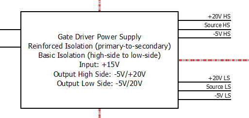
I’m designing an inverter gate driver power supply for a client and looking at the following arrangement. I’m looking at using a no-opto flyback supply with a custom transformer to generate all the required voltages. However, I normally see the gate supply for the upper and lower MOSFET’s separated i.e. separate gate supplies with separate transformers and I was curious to know why it’s implemented in this fashion.
The only reason I can think of is noise coupling issues or perhaps safety. However, the latter would not apply with a sophisticated gate driver IC like the MC33GD3100. I understand the capacitance between secondaries (and the primary) needs to be as small as possible (in the pF range).
Given that you liaise with many engineers and work on many projects, do you have any thoughts on this?
Answer:
Isolated supplies are usually used where either the control circuit is at a safe potential (for galvanic isolation purpose)or where the output needs to get to 100% or 0% duty cycle or both (0-100%). For instance, large industrial motor drives I have seen always have isolated supplies so that the modulation index can go very high. Think about even more advanced PWM methods such as DPWM, SVM, you have periods where the modulation index needs to go either 0 or 100%. This is the same for high power SMPS, where you want to get the largest control range.
The isolated supplies can either be separate windings on a flyback or a central oscillator with separate transformers. Generally speaking, transformer coupled gate drives are more robust than opto isolators or level shifters for the high dV/dt that you often get on the upper driver (when I was a motor drive engineer designing driver circuits, I noticed the upper switching has much higher dV/dt due to a few factors, you know, the usual suspect, miller capacitance of the bottom device, the body diode reverse recovery charge, dead time, etc). So, if you need an equally balanced upper and lower drive, you can have a transformer with a single primary and two secondaries. One for the lower gate drive and one for the upper drive. There’s no issues with this as far as I know. So I don’t know why you mentioned one supply for one drive for most designs you saw. In my opinion, there’s no significant technical barrier to discourage people from doing the single supply design. To me, it is also not wise to do separate power supply design as first, it results in a not-so-good form factor, second, it leads to more cost.
Another good thing about transformer supply is that they are almost immune from fast transient bursts (unless, as you pointed out, they have very big parasitic capacitance between the primary and secondary stage).
So I basically agree with you, I don’t think there’s anything that stops you doing a design that has one supply from safety and EMC point of view. In terms of performance, as long as you have a good transformer design and good control of the switchers, I simply cannot see why not. This is particularly true if you have a phase-shift full bridge converter for instance.
Feedback
I contacted another engineer who has worked on the layout of an inverter (not the design) and his response was,”It seems like using two separate flybacks is compulsory for safety reasons alone.
I believe it is a requirement that the high and low side must be isolated for DFMEA considerations if there is a breakdown, say between the gate and the source of either high or low side. I also understand that immunity in a noisy environment like where this would be installed also plays an important role, I guess with things like avoiding the back EMF of each side avoiding coupling onto the other.”
My concerns would lie in potential coupling issues between the high-side and low-side due to the capacitance between the windings of the gate driver transformer. In terms of safety, the gate driver IC that I’ve selected should shut down safely in an event where the high-side and low-side supplies suddenly collapse. In terms of voltage breakdown, I normally use triple insulated wire or FIW for this type of application which provides reinforced isolation however, a breakdown could theoretically still occur albeit very low.
Moving forward, I have decided to use individual gate driver transformers for this application.