Shall I use wire connection or PCB connection?
From: Steve, Power Electronics Lead, United Kingdom
Question: During our product development stage, we had a query regarding whether it’s better to use a PCB to connect two other PCBs or cables? Sometimes, there’s no choice but to have two physically separated PCBs for eg control and power and we’ll have a bit of space to run a cable or a joining PCB. Would you recommend a cable or a pcb with board to board connectors in the situation for EMC repeatability? In both cases they would have some signals and low voltage supplies.
Answer:
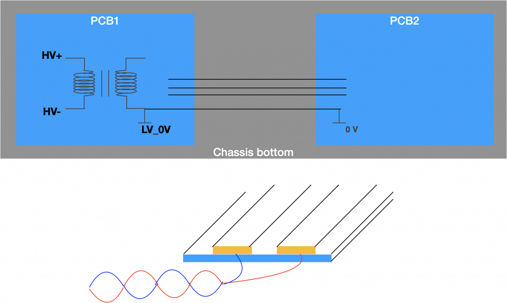
Imagine we had two PCBs joint as one, you would carefully designed the 0V, power and signal routing so that the signal integrity and power integrity are controlled. If this is controlled, there is less EMI issue in general.
But obviously, with 2 PCBs, we had issues with interconnections. There is a phenomenon called “Mode Conversion (DM TO CM)”. Mode conversion occurs when there is a change in the electrical balance of the signal carrying conductors. So at the point of the change in the balance, a common-mode voltage is created. And we all know that a common mode voltage is the culprit for emissions.
Dr Todd Hubing is an expert in this specific area and I highly recommend his works on this subject. Here we quote what he said
‘A discontinuity in the ground structure could produce mode conversion if it changes the balance of the transmission line.’
So the key point here is BALANCE. Here is again from Todd, ‘Suppose a differential signal is propagating on a pair identical traces above a ground plane (as shown in the picture). If the signal leaves the board on a twisted pair leaving the ground plane behind, there is no conversion from DM to CM as long as the trace pair and the twisted pair were both balanced. In another case, say a power trace is routed over the top of the ground plane leaves the board and connected to a twisted pair, there will be mode conversion.’
If you use a PCB to connect the two boards, you still have the challenges of connecting both ends of the PCB. The “Ground” difference depends on the inductance, and the inductance does not care if the link is a fat wide cable or a thin wire, it is the loop area that is the key. In both cases, the loop areas are the same.
If both PCBs have good connection to chassis bottom, so that the “Ground (0V)” difference between the two is small, you significantly reduce the noise.
To me, you can use wire connection if you follow the guidance below:
- Separate power lines and signal lines. For signal lines, as mentioned before, keep the trace on the board balanced and keep the signal line on the wire balanced (you don’t need twisted pair most of the time).
- Avoid using ribbon cable.
- If you can twist power and gnd, that is good.
- For power and gnd line, you can place a filter at the connector side, a C-L-C filter on one board is perhaps enough.
If you use PCB, the principle is exactly the same. But pay attention to PCB to PCB connections as you change from one transmission line (on PCB1) to the intermediate wire(possibly), then to the link PCB and then wire and PCB. If you have continuous trace on the PCB (like those flexible PCBs often seen in cameras, sat-nav, etc), obviously that is good, but I don’t see how we can implement in your application.