By Min Zhang, the EMC Consultant
Many of the self-employed engineers or electronics hobbyists enjoy making DIY tools. Not only do these self-made tools beat the price of a commercially available product down significantly, but more importantly, by making these tools, one can generally learn a lot. Most important of all, the fun of making things just cannot be described.
This article is based on existing works presented by Doug Smith[1]-[3], and many others[4]-[5]. The process of making these probes are described in details in these articles. Therefore, we only cover some of the points that are not covered by these articles, these points could be very important to make the probes work. Tests of these probes are also introduced in this article.
To make a balanced voltage probe as described in [1], one needs to make two resistive voltage probes which are matched (to the frequency range required). This is very important for the balanced probe to work as difference between the probes will reduce the Common-mode Rejection Ratio (CMRR) by a lot. Two resistive probes were made based on the step-to-step manual in [2]&[3]. In this case, four 200 Ω resistors were constructed in parallel to create the 50 Ω feedthrough, and one 750 Ω resistor was used as the tip resistor. This means, a single probe would give 31× ratio (~30dB) measured on a 50 Ω impedance (spectrum analyser or the 50 Ω input of an Oscilloscope). A balanced probe (consisting of two of these probes, plus the splitter) will give a 50× ratio (~34dB)[1].
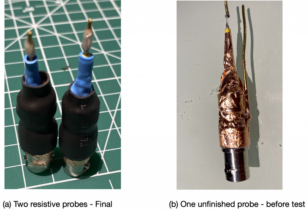
Using the techniques introduced in [2][3], two resistive probes are made and shown in Figure 1. On the left are the final probes (with heat shrink and without ground leads). On the left shows one probe before the final stage (without heat shrink and with ground lead). Also note that the final probe has front end resistor tip glued using e-poxy, this gives extra protection for the probe tip, as it was found during the test that the tip is prone to be broken (since a surface mounted 1206 resistor is used, a through hole resistor is more robust, but could potentially introduce more ringing due to the ESL). But before putting on the heat shrink and epoxy, the two probes need to be tested to make sure their frequency response are the same.
The probes are tested using a spectrum analyser that has a tracking generator function. In this case, a Siglent SSA 3021X is used. Note that the final balanced probe also use a pair of identical 50 Ω co-axial cable, so the first is to test the characteristics of the pair of cables. The cables that are used for making the balanced probes are TE Connectivity BNC male to BNC male, 500 mm long coaxial cables. They show exactly the same impedance characteristics.
To test the probes. Set the TG output as -10dBm. Use the probes to measure the output of the TG source directly. Obviously, this measurement is rather rudimental as a network analyser using Kelvin bridge would be much accurate, but since we are only comparing the difference of the two probes, this method is acceptable. One can either use the linear scale or log scale, here we use the log scale. The frequency range is set between 1 MHz and 1 GHz.
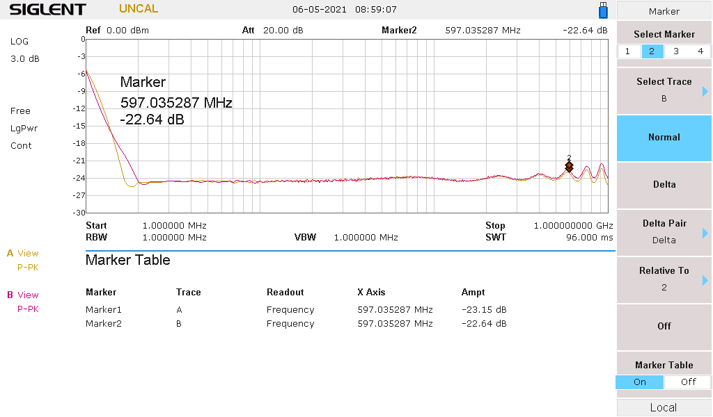
It can be seen from the result that the two probes matched well till about 600 MHz. From 600 MHz upwards to 1 GHz, the difference between the two becomes bigger. There are a few techniques that can be used to bring down the difference, which we will discuss in a separate article. But for now, we are happy with the matching of the two probes. The reason is simple, my oscilloscope is 500 MHz bandwidth, the splitter I use is also 500 MHz, so there’s really no need to fine tune the probe from 500 MHz to 1 GHz.
Notice, the attenuation shown in the test is about -23dB, not the -30dB we expected, why? We will leave this question to our readers. And the answer can be found in a separate article here.
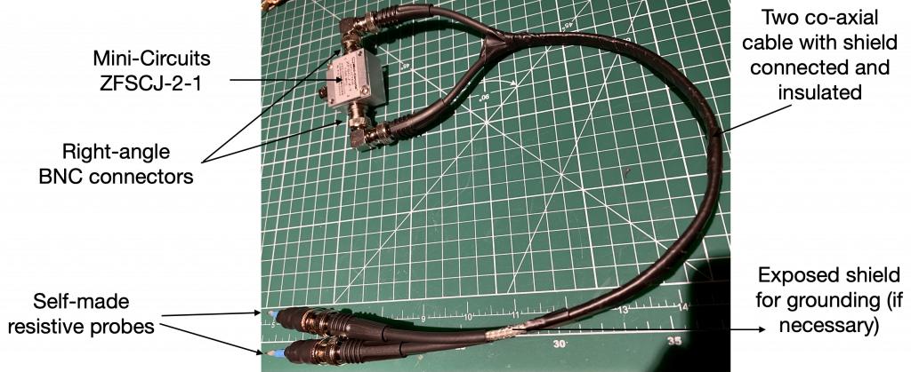
Once the two probes are tested to be matched well. Heat shrinks are added. As mentioned previously, e-poxy is used to fasten the probe tip to avoid accidental damage. Following the instructions in [1], the final balanced probe is shown in Figure 3.
The probe needs to be tested to see if its performance is up to what we expected. The test setup is simple. Use a functional generator (Aim-TTi TGF 4242) to generate a 20 MHz, 3.9 Vpp (50Ω load), square wave. Rise time is fixed as 4ns. The reason to use 3.9 Vpp is because the rise time is slightly faster when Vpp is less than 4V. Measurement is shown on Rigol MSO5204 (this is an old oscilloscope which I had it upgraded to 350 MHz, my new 500 MHz scope is out for work currently. This model does not have the 50 Ω input impedance option, therefore, a 50 Ω feedthrough terminator is used on the BNC input of the oscilloscope.)
As it can be seen from Figure 4, the balanced probe does provide a much better waveform compared with the 350 MHz High Impedance Probe. Figure 4 (a) shows the result by directly connecting the BNC cable into the oscilloscope (using 50 Ω feedthrough termination). This serves as a reference, in reality, this cannot be used as a practical way of measuring circuit. The balanced probe has a 50× ratio (0.16 Vpp/7.8Vpp=0.02).

Further Improvement
Further improvement can be made to enhance the performance of the balanced probe. This includes
- To improve matching between the two probes till 1 GHz.
- There are oscillation observed from the resistive probe (single one) from 500 MHz, this could be due to the L-C resonance introduced by the construction. So far, I have not figured out how to reduce the oscillation and make the attenuation curve a flat straight line.
- The split tip of the balanced probe is less than 10 cm, making the opening angel very small, it might be worth extending the length of the split part so as to make measurement easy.
Equipment List
The equipments mentioned in this articles are:
- Siglent SSA 3021X spectrum analyser, 9kHz-2.1GHz, with Tracking Generator option.
- Rigol MSO5204 digital oscilloscope, with bandwidth upgraded to 350 MHz.
- 50 Ω feed-through terminator, CT2944C-50, which claims to work till 1 GHz, but I found these 50 50 Ω feed-through are not so great above 500 MHz, though I never used very expensive ones to compare.
- Aim-TTi 240 MHz TGF4242 function generator, minimum rise time is 3 ns.
- Mini-Circuits splitter ZFSCJ-2-1 1-500MHz.
- 3×TE Connectivity BNC male to BNC male 50 Ω coaxial cable, 500 mm long
- 2 BNC barels to make the resistive probes
- 200 Ω resistors, 1206; 750 Ω resistors, 1206.
- Brass wires
Reference:
[1] D.C. Smith, Balanced Probe Extends High-Frequency Measurements, IEEE Circuits & Devices, Vol.10, No.6, pp 19-23, November, 1994, http://emcesd.com/pdf/cd94scr.pdf
[2] D.C. Smith, DC to 1GHz Probe Construction Plans, November 1, 2004, http://emcesd.com/1ghzprob.htm
[3] D.C. Smith, Improved Construction Techniques for a 50 Ohm Termination, http://emcesd.com/tt030100.htm
[4] J. Kapsi, A wideband 1:21 DIY 1 kOhm Oscilloscope Probe, http://jahonen.kapsi.fi/Electronics/DIY%201k%20probe/
[5] Paul, Praise for the Lo-Z Probe. Lessons in High-speed Probing, http://paulorenato.com/index.php/electronics-diy/93-praise-for-the-lo-z-probe