By Dr. Min Zhang, the EMC Consultant
Download link is provided below
Background
A switched mode power supply (SMPS) which uses a ‘silent switcher’ and has a designed filter capable of more than 60 dB attenuation in the frequency range of 500kHz to 30 MHz failed conductive emission test. The SMPS has a fixed frequency of 1.8 MHz, as a result, the harmonics of 1.8 MHz spikes were seen everywhere in the spectrum, indicating the noise spreads over the PCB and the filter has little effect.
Why is that the case?
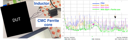
Stage 1 Investigation – Ferrite core approach
It is always a relatively easy approach to use ferrite cores to help us trouble shooting. In this case, we suspected the noise contains both differential-mode and common-monde contents. Therefore, we used a 33μH inductor followed by a ferrite-core (44 material, which is effective from 25MHz to 300 MHz) common mode choke. As explained in many of our materials before, in the low frequency range, the noise is predominantly differential-mode, as frequency increases, the common-mode noise becomes more dominant.
As shown in Figure 1, the added filter configuration on the power line reduced the noise from 150kHz to 30 MHz.
We need to understand where does the noise come from.
Stage 2 Investigation – Near-field probing approach
By using a magnetic field probe across the PCB, we identified that the noise comes from the SMPS area. It is a step-down converter that has rated 20A output current. So one could expect that if the design is not done properly, leakage field will couple to the nearby circuits and pollute the PCB.
In Figure 2, we probed three locations on the shielded inductor in the SMPS. Note that the hot node of the inductor has the largest amplitude of noise.
This shielded inductor is the output inductor, with one end connected to the switch node of the SMPS chip, and the other connected to the output capacitor. The hot node of the inductor is the noise source. In this case, the shielded inductor didn’t shield the field as intended. As a result, noise is ‘leaking’!
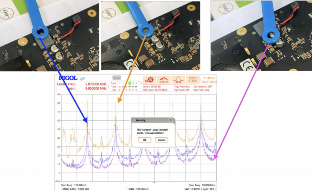
The reason that this switch node is leaking is because the copper area of this switch node is very large on layer 1. As a result, the shield cannot cover the whole switch pad. Leakage flux is then coupled to the input stage filter of the SMPS, making the input stage filter almost useless.
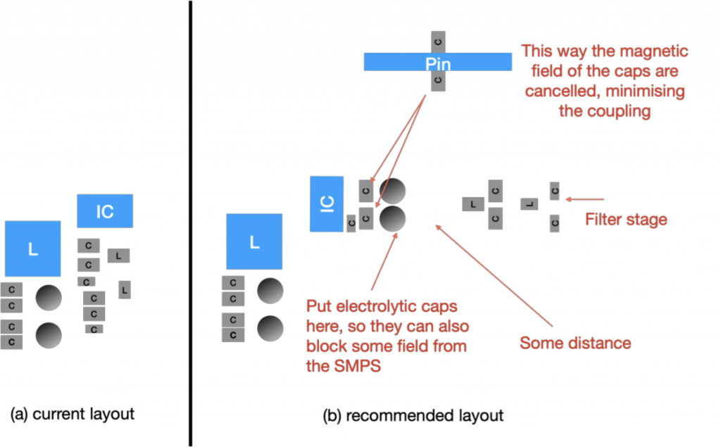
Another big issue of this SMPS design is that input filter and output filter are in parallel on the PCB and they are very close, which means that the input filter is bypassed due to the strong coupling of the input and output. It is very similar to another common mistake seen in the industrial application where engineers put a filter in a container very close to the noise source. A filter is effective when it is away from the noise source. So in this case, we need to separate the input and output filter, like what is shown in Figure 3.
Stage 3 Investigation – Prove the concept
We need to demonstrate the point to convince the engineers and their managers. But layout work is never easily done with limited given amount of time. So we shielded the output filter and compared the conducted emission result with the previous result. As it can be seen in Figure 4, shielding the output stage reduces the noise by about 20dB across a wide frequency range.
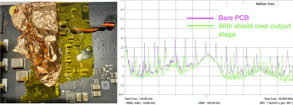
To apply the shield effectively, first put a Kapton tape on the area of interest. Then put copper tape on top of the filter, make sure the whole area is fully covered and finally connect the copper tape to a ground. Luckily enough, there’s a gnd ring next to the inductor, which enabled us to ground the shield.
Conclusion
The input stage filter of a step-down converter is crucial for passing the EMC. Not only do you need to show good attenuation in the simulation, but also you need to lay out the filter properly. General rules are:
- Keep the input stage filter away from the SMPS, better put it on the other side of the PCB.
- Make sure the coupling mechanism between the input stage and output stage of a SMPS is kept minimum by applying proper layout.
- Always check the hot nodes, make sure they are well contained.